 首頁/ 最新消息
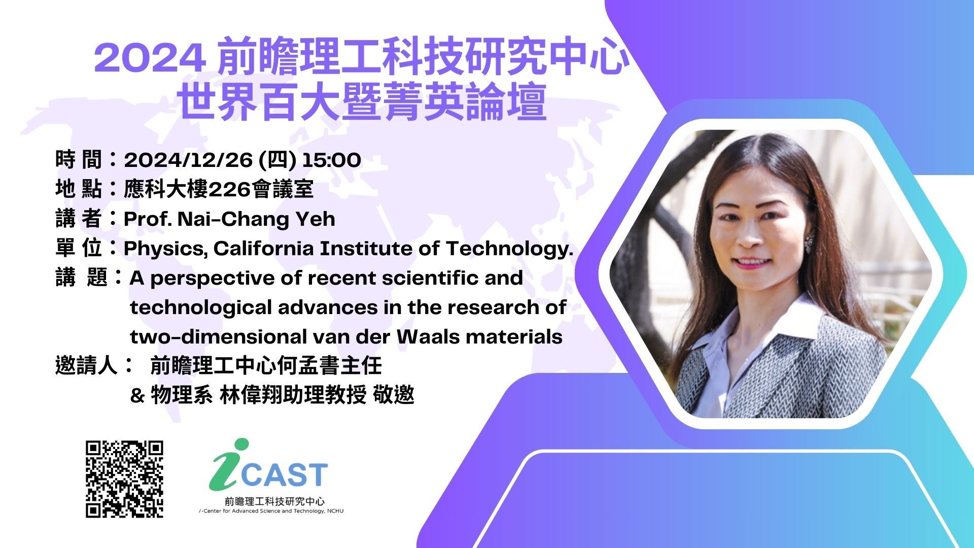
12/26 (四)Global Top 100 and Elite Forum: Prof. Nai-Chang Yeh 講題: A perspective of recent scientific and technological advances in the research of two-dimensional van der Waals materials
時 間:2024/12/26 (四)15:00
地 點:應科大樓226會議室
講 者:Prof. Nai-Chang Yeh
單 位:Physics, California Institute of Technology. (加州理工)
講 題:A perspective of recent scientific and technological advances in the research of two-dimensional van der Waals materials
邀請人:前瞻理工中心 何孟書主任 & 物理系 林偉翔 助理教授 敬邀
Time: 3pm December 26, 2024 (Thursday)
Place:2F 226 meeting room ,Applied Science & Technology Building, NCHU
Speaker:Prof. Nai-Chang Yeh
Physics, California Institute of Technology
Title:A perspective of recent scientific and technological advances in the research of two-dimensional van der Waals materials
Host by:Director, Prof. Mon-Shu Ho & Prof. Wei-Hsiang Lin
報名連結:
https://icast.nchu.edu.tw/activity.php?id=2de2647c-ab08-11ef-b6c5-56000176fdd3
Abstract:
Two-dimensional (2D) van der Waals (vdW) materials, such as graphene, hexagonal boron nitride (h-BN) and transition metal dichalcogenides (TMDs), are quantum materials exhibiting a rich variety of properties that are not only exciting for scientific research but also promising for a wide range of technological applications. In this talk I will first summarize the recent developments in my group on graphene-based technologies, including flexible electronics, interconnects, anti-corrosion for biomedical and photovoltaic applications, superlubricity, and photonics. [1] These studies are all based on graphene synthesized by scalable, reproducible, and industrially compatible method of plasma enhanced chemical vapor deposition (PECVD). [2,3] Next, I will describe four topics of our scientific studies based on vdW materials, which include 1) straintronic devices based on nanoscale strain engineering of monolayer graphene that exhibit strain-controlled emerging quantum phenomena; [1,4] 2) topological photonics based on monolayer TMDs, plasmonic metasurfaces, and topological light (i.e., photons with nontrivial spin or orbital angular momenta); [5,6] 3) giant ferroelectric and optoelectronic responses from field effect transistors made of monolayer TMDs; [7] and 4) light-induced dramatic renormalization of the electronic density of states in strained monolayer TMDs and its potential application to solid-state quantum simulators. [8] Finally, I will discuss the outlook of developing scalable and CMOS compatible synthesis of monolayer and few-layer 2D-TMDs, which will be critically important for realizing the full technological potential of TMDs.
References:
[1] “A perspective of recent advances in PECVD-grown graphene thin films for scientific research and technological applications”, C.-H. Lu, D. Hao, and N.-C. Yeh*, Materials Chemistry and Physics 319, 129318 (2024); and references therein.
[2] “Single-step deposition of high-mobility graphene at reduced temperatures”, D. A. Boyd, W.-H. Lin, C.-C. Hsu, M. L. Teague, C.-C. Chen, Y.-Y. Lo, W.-Y. Chan, W.-B. Su, C.-S. Chang, Chih-I. Wu, and N.-C. Yeh*, Nature Communications 6, 6620 (2015).
[3] “Single-step direct growth of large-area graphene and graphene-based nanostructures on silicon for ultra-low-friction and potential optoelectronic applications”, Wei-Shiuan Tseng, Yun-Chun Chen, Chen-Chih Hsu, Chih-I Wu and N.-C. Yeh*, Nanotechnology 31, 335602 (2020).
[4] “Nanoscale engineering of giant pseudo-magnetic fields, valley polarization and topological channels in strained graphene”, C.-C. Hsu, M. L. Teague, J.-Q. Wang and N.-Chang Yeh*, Science Advances 6, aat9488 (2020).
[5] “Dramatically enhanced valley-polarized emission of monolayer WS2 at room temperature with plasmonic Archimedes spiral nanostructures and gated control”, W.-H. Lin*, P. C. Wu, H. Akbari, G. R. Rossman, N.-C. Yeh* and H. A. Atwater*, Advanced Materials 34 (3), 2104863 (2022).
[6] “Control of trion-to-exciton conversion in monolayer WS2 by orbital angular momentum of light”, R. Kesarwani, K. B. Simbulan, T.-D. Huang, Y.-F. Chiang, N.-C. Yeh*, Y.-W. Lan* and T.-H. Lu*, Science Advances 8, eabm0100 (2022).
[7] “Magnetic field-induced giant electric hysteresis in monolayer MoS2 transistors”, D. Hao, W.-H. Chang, Y.-C. Chang, Y.-C. Chang, W.-T. Liu, S.-Z. Ho, C.-H. Lu, T. H. Yang, N. Kawakami, Y.-C. Chen, M.-H. Liu, C.-L. Lin*, T.-H. Lu*, Y.-W. Lan* and N.-C. Yeh*, Advanced Materials 2411393 (2024).
[https://doi.org/10.1002/adma.202411393]
[8] “Strongly enhanced electronic bandstructure renormalization by light in nanoscale strained regions of monolayer MoS2/Au(111) heterostructures”, A. Park, R. Kantipudi, J. Göeser, Y. Chen, D. Hao, and N.-C. Yeh*, ACS Nano 18 (43), 29618-29635 (2024).


